Custom Processing of LVDS Wiring Harness
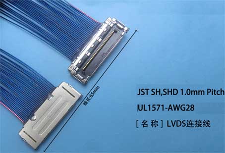
LVDS low-voltage differential signaling is a differential signaling technology with low power consumption, low bit error rate, low crosstalk and low radiation. The LVDS wiring harness is the bridge channel between the display screen and the communication motherboard. It plays the role of power supply and signal transmission, and the main board transmits the picture to the display screen. This transmission technology can reach more than 155Mbps. The core of VDS technology is to use extremely low voltage swing to transmit data at a high speed, which can realize point-to-point or point-to-multipoint connection. The transmission medium can be a copper PCB connection or a balanced cable
Commonly used wires such as: UL1571-AWG28 wire (the larger the number, the thinner the wire).
Technology Brief
LVDS is a low-amplitude differential signal technology. It uses very low amplitude signals (about 350mV) to transmit data through a pair of differential PCB traces or balanced cables. It can transmit serial data at speeds up to thousands of Mbps. Because the voltage signal amplitude is low and it is driven in a constant current source mode, it only generates extremely low noise, consumes very little power, and even the power consumption is almost unchanged regardless of the frequency. In addition, because LVDS transmits data in a differential manner, it is not susceptible to common mode noise.With the continuous advancement of electronic design technology, the interconnection of high-speed signals and the application of broadband channels are increasing day by day, and the amount of data that needs to be transmitted is increasing and the speed is getting faster and faster. At present, the existing point-to-point physical layer interfaces such as RS-422, RS-485, SCSI and other data transmission standards are inherently limited in terms of speed, noise, EMI/EMC, power consumption, and cost. Make it more and more difficult for practical applications. Also with the development of military electronic technology and the field of space communication: Such as tracking and data relay satellite system (TDSS), in order to achieve high-speed data relay and ranging, speed measurement. The problems caused by high transmission rate and occupied bandwidth must be solved first; In the field of radar applications, the emergence of various new systems of radar and applications in different fields such as broadband reconnaissance and electronic countermeasures also inevitably face high-speed data acquisition and transmission problems; Therefore, the use of new I/O interface technology to solve the bottleneck problem of data transmission has become increasingly prominent. With its inherent low voltage, low power consumption and high-speed transmission characteristics, LVDS has increasingly become the preferred interface standard for broadband high-speed system design. At present, the application of LVDS technology in the communication field is becoming more and more popular, especially in base stations, large switches and other high-speed data transmission systems, LVDS is playing an irreplaceable role.
The basic principle of LVDS wiring harness
The basic working principle of LVDS is shown in Figure 1. The source driver consists of a constant current source (usually about 3.5mA, the maximum is not more than 4mA) driving a pair of differential signal lines. The receiver at the receiving end has a high DC input impedance, so almost all of the drive current flows through the 100Ω terminal matching resistance, and a voltage of about 350mV is generated at the input end of the receiver. When the driving state of the source terminal is reversed and changed, the direction of the current flowing through the matching resistor changes, so that a high and low logic state change occurs at the receiving terminal.In order to adapt to the wide-range variation of the common-mode voltage, in general, the LVDS receiver input stage also includes an automatic level adjustment circuit, which adjusts the common-mode voltage to a fixed value; Behind it is a Schmitt flip-flop, and, in order to prevent the Scdhmitt flip-flop from being unstable, the design has a certain hysteresis characteristic, and the Schmitt rear stage is a differential amplifier.
Technical characteristics
The reason why LVDS has become the preferred signal form of the current high-speed I/O interface to solve the limitations of high-speed data transmission is because it has advantages in transmission speed, power consumption, noise resistance, and EMI.① High-speed transmission capability. In the LVDS standard defined in ANS/EIA/EIA-64, the theoretical limit rate is 1.923Gbps. The working mode of constant current source mode and low swing output determines the high-speed driving capability of IVDS.
② Low power consumption characteristics. LVDS devices are implemented using CMOS technology, and CMOS can provide lower static power consumption; When the driving current of the constant current source is 3.5mA, the power consumption of the load (100Ω terminal matching) is only 1.225mW; The power consumption of LVDS is constant, unlike the dynamic power consumption of CMOS transceivers that rise with respect to frequency. The drive design of the constant current source mode reduces the power consumption of the system and greatly reduces the influence of frequency components on the power consumption. Although the power consumption of CMOS is lower than that of LVDS when the speed is lower, as the frequency increases, the power consumption of CMOS will gradually increase, and eventually it will need to consume more power than LVDS. Generally, when the frequency is equal to 200MSps, the power consumption of LVDS and CMOS is roughly the same.
③ The power supply voltage is low. With the development of integrated circuits and the requirement for higher data rates, low-voltage power supply has become an urgent need. Reducing the power supply voltage not only reduces the power consumption of high-density integrated circuits, but also reduces the heat dissipation pressure inside the chip, which helps improve integration. LVDS drivers and receivers do not depend on specific power supply voltage characteristics, which determines that it occupies the top in this regard.
④ Strong anti-noise ability. The inherent advantage of differential signals is that noise is coupled to a pair of differential lines in a common mode, and subtracted in the receiver, so that noise can be eliminated. Therefore, LVDS has a strong ability to resist common mode noise.
⑤ Effectively suppress electromagnetic interference. Since the polarities of the differential signals are opposite, the electromagnetic fields radiated by them can cancel each other out. The tighter the coupling, the less electromagnetic energy is released to the outside world, which reduces EMI.
⑥ Precise timing positioning. Because the switch change of the differential signal is located at the intersection of the two signals. Unlike ordinary single-ended signals, which rely on high and low threshold voltages to judge, they are less affected by process and temperature, which can reduce errors in timing and facilitate the effective transmission of high-speed digital signals.
⑦ Adapt to the large voltage variation range of the ground plane. The LVDS receiver can withstand a voltage change between the driver and the receiver of at least ±1V. Since the typical bias voltage of the IVDS driver is +1.2V, the sum of the ground voltage change, the driver's bias voltage, and the lightly coupled noise, is a common-mode voltage at the receiver input relative to the driver's ground. When the swing does not exceed 400mV, the common mode range is +0.2V~+2.2V, and in general, the input voltage range of the receiver can vary from 0V to +2.4V.
It is precisely because LVDS has the above-mentioned main features: This makes HyperTansport (by AMD), Irfiniband (ly Intel), PCI-Express (by Intel) and other third-generation I/O bus standards (3G IO) coincidentally use low-voltage differential signaling (IVDS) as the next generation of high-speed signal levels standard.
Technology Application
In the field of radar applications, with the development of technology, new system radars such as DBF system radars, phased array radars, etc. have appeared and popularized. The signal bandwidth and the number of signal channels that need to be processed have greatly increased, and the problem of large data volume transmission is faced. Therefore, it has become an inevitable trend to adopt new technologies to solve the I/O interface problem. LVDS, a high-speed and low-power interface standard, makes it possible to solve this transmission bottleneck problem. Therefore, LVDS technology is currently widely used in high-speed radar and high-speed receiving systems; Using LVDS technology to realize point-to-point single board interconnection, the system structure is very extensible, and the high integration of line cards and various sub-systems is realized, and it can fully meet the requirements of data collection and transmission.In civilian use, this technology can support high-speed data transmission. It is most suitable for communication structure applications such as base stations, switches, plus/minus multiplexers, application solutions for consumer products such as set-top boxes and home/enterprise video links, as well as medical ultrasonic imaging equipment and digital photocopiers. Ensure that the partition operation of the system can exert greater flexibility. System design engineers can use LVDS technology to set the analog and digital signal processing sections on different circuit boards, and then use cables or backplanes to transmit the digital data output by the A/D converter to ensure greater flexibility in structural design. At present, all types of high-speed AD converters basically choose to use LVDS signals as the output format of sampled data, and most of their output forms are parallel output. At the same time, dedicated chips supporting IWDS and other level interchange and dedicated LVDS speed reduction chips are also emerging in an endless stream, mainly represented by several foreign companies such as MAXM, NI, and TI.
In addition, LVDS has a very broad application space in the applications of high-speed data transmission, SAR radar reconnaissance and reception and high-speed digital image transmission of measurement and control systems. Especially in recent years and in the next few years, the aerospace, military, communications and other sectors have continued to increase their demand for flexible high-bit-rate communication systems. On the one hand, the core of the traditional communication system, filters, mixers and other links are mostly realized by analog devices, which greatly restricts the reliability, flexibility, upgrade and maintenance of the system. On the other hand, in the past 20 years, the rapid development of microelectronics technology, integrated circuits, and digital communication theory has made it possible to implement many links in a high-bit-rate communication system using digital methods. According to the information obtained so far, foreign countries have successfully developed a variety of high-performance, flexible and versatile all-digital high-bit-rate baseband signal processors. At present, we have made major breakthroughs in the research process of high bit rate digital transmission technology, and one of the key technologies applied is LVDS technology.


